PCBA
  • What is the PCB metal edging?
    August 12, 2021 What is the PCB metal edging?
    There are 2 types of printed circuit boards for PCB circuit boards, one with non-metallic edges and the other with metalized edges. In the past, there was not much demand for PCBs with metal edges, and now there are more customer demands. Higher-quality printed circuit board metal edges have attracted more attention because it enhances the functionality of several products that use these printed circuit boards. With the miniaturization and high-speed operation of circuits, the timing and signal integrity of digital signals have become prominent issues. In addition, due to the integrity of the power supply, the medium and high speed digital signals in the system will cause electromagnetic interference and electromagnetic compatibility problems. High-speed digital signals will not only cause serious interference inside the system, but also radiate to the outside of the system, causing the equipment to exceed the safety limit standards. The side-board radiation of a multilayer PCB is a relatively common source of electromagnetic radiation. The current-carrying power layer and ground layer will generate electromagnetic radiation at its edges. Due to insufficient power supply bypass, most of the noise comes from stray currents in the power and ground planes. At high frequencies, vias act as stubs and may have high inductance. This kind of through hole can radiate the magnetic field between the layers of the circuit board, and finally gather at the edge. The PCB board metallization edge process uses metal to surround the entire board edge. This will short-circuit the high-frequency signals reaching the edge of the circuit board and prevent them from radiating. Although this improves the performance of the circuit board, the edge metallization process increases the cost of the printed circuit board.
    View More
  • What is different between FPC(Flexible printed circuit board) and FFC(Flexible Flat Cable)?
    July 24, 2021 What is different between FPC(Flexible printed circuit board) and FFC(Flexible Flat Cable)?
    1. Different materials: FFC is composed of PET insulation material and extremely thin tinned flat copper wire. FPC is composed of copper foil, acrylic & epoxy resin thermosetting  adhesive and Polyimide film. 2. Different manufacturing methods: FPC processes the flexible copper clad foil by chemical etching to obtain flexible circuit boards with different shapes of single-sided or double-sided and multi-layer structures.FFC is a flat copper foil sandwiched between the upper and lower insulating foil films, which are pressed together through the production line of high-tech automated equipment. The finished product is simpler and thicker. 3. Different applications: FPC can carry out impedance control, anti-static interference, designed to have bending and angle, commonly used in FPC antennas, FPC touch screens, FPC capacitive screens, notebooks, SLR cameras, smart phones, wearable devices, automotive electronics, medical equipment, industrial control equipment, Military equipment, sensors, antennas and other modern electronic products. FFC is easy to solve electromagnetic shielding (EMI). It is often used in the connection between the print head of the printer and the motherboard, plotters, scanners, copiers, audio, LCD appliances, fax machines, various DVD players, etc., PCB board to PCB board It is used as data transmission cable in miniaturized electrical equipment.
    View More
  • The meaning of PCB board for graphics card
    July 12, 2021 The meaning of PCB board for graphics card
    The graphics board refers to the PCB circuit board on the graphics card. It can also be called the graphics card motherboard, because the graphics card is composed of a heat sink + GPU + video memory + circuit board + other components. The components of the graphics card are all placed on the PCB board. Good or bad, directly determines the quality and stability of the electrical performance of the graphics card. The PCB board is the basis of the graphics card. The more PCB layers, the more complex the design, the more precise the workmanship, and the better the overclocking and stability. The PCB board not only supports the components of the entire graphics card, but also plays a vital role in the stability of the graphics card. It is the soul of the quality of the graphics card. At present, motherboards and graphics cards mostly use multi-layer boards, which greatly increases the area that can be wired. However, based on cost considerations, six-layer or four-layer board designs are generally used, and only a small number of high-end graphics cards use eight-layer board designs. With the gradual maturity of the current PCB industry, the GPU industry is bound to usher in new developments.
    View More
  • Why does PCB have a craft edge?
    July 07, 2021 Why does PCB have a craft edge?
    In the process of SMT patch processing, the PCB is completed by track transmission. The PCB board needs to be fixed during track transmission. Conventional equipment uses the splint method and there should be no components and parts in the clamped range and the crawler range. Lead interference, otherwise it will affect the normal transmission of the PCB board due to the inability to clamp and fix, or reduce the work efficiency due to the collision of the patch parts and the equipment too close. Therefore, it is necessary to add some blank areas on both or four sides of the PCB as process edges, reserve a safe distance, and expand the space from the patch parts in the PCB to the edge of the board to assist PCB production and processing. The reserved width of the craft side is generally recommended to be 5.0mm.   However, not all PCB boards need to add process edges. If the space between the patch parts in the PCB board and the board edge is large enough and not within the crawler range, there is no need to add additional process edges.
    View More
  • PCB via analysis
    June 23, 2021 PCB via analysis
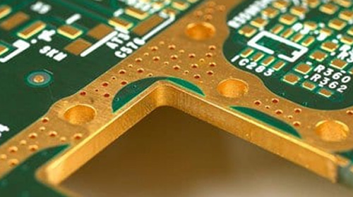
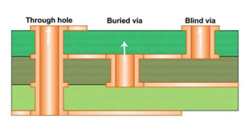
    Every hole on the PCB can be called a via. It is one of the important components of multilayer PCB. Let's get to know the knowledge of vias together. Drill a common hole, that is, a via hole, at the intersection of the wires that need to be connected to each layer of the double-sided or multi-layer board. In terms of function, it is used as the electrical connection between the various layers of the PCB; and the other is used as the fixation or positioning of the device. In terms of process, via holes are divided into three types: blind holes, buried holes, and through holes. Blind holes are through holes that connect the surface and inner layers without going through the entire board, and are used to connect and conduct two or more layers of PCB. The copper foil lines between, because all the layers are not drilled, only the top layer or the bottom layer can be seen. Buried holes are connecting holes in the inner layer of the PCB. They are used to interconnect any circuit on the inner layer, but they do not extend to the surface of the circuit board, so the surface and bottom layers are invisible. There is also a through hole, which passes through The whole PCB can realize the conductive connection between different layers or the installation and positioning of components. In the design of vias, the size, quantity and spacing of vias must be designed after comprehensive consideration and the manufacturing process, structural reliability, performance and other issues must be taken into account. For example, factors such as current and wiring must be considered. For some high-speed or high-density products, the smaller the via hole is the better, so that more wiring space can be reserved on the board, thereby increasing the wiring density. In addition, the smaller the via hole, the smaller its own parasitic capacitance, which is more suitable for high-speed circuits. However, limited by technology such as drilling and electroplating, the smaller the hole, the longer it takes to drill and the easier it is to deviate from the center position. And when the depth of the hole exceeds 6 times the drill diameter, the hole cannot be guaranteed The wall can be plated with copper uniformly. For the vias of the power supply or the bottom line, consider a larger size to reduce the impedance, and drill multiple holes in parallel to reduce the equivalent inductance. The spacing between vias and vias should also be avoided. If the spacing is too small, it is easy to cause holes when drilling.
    View More
  • What is flying probe testing
    June 17, 2021 What is flying probe testing
    There are many test methods in PCBA processing plants, among which flying probe test and needle bed continuity test are more common test methods, they are all a kind of contact test, and flying probe test is an improvement of needle bed continuity test Upgraded version. Flying probe test (FPT) is an automated test that uses a movable probe to replace the traditional fixed needle bed fixture and adds a probe drive device. In this test, two or more probes are programmed to move, and access various component pins one by one to detect whether there are open circuits, short circuits, and component value parameter errors. Since flying probe probes need to be programmed for each PCB board type, which takes a long time, PCB boards are usually suitable for prototype and small-batch PCB testing. Flying probe test has the following advantages: 1. Since the flying probe test is supported by software, it is easier for engineers to get feedback in time in case of errors. 2. The flying probe tester is equipped with a camera to identify missing components. 3. The flying probe probe can be easily moved from one node to another, with strong precision and accuracy. 4. Flying probe test does not require fixture development, which saves test costs. Flying probe detection is currently mainly used in industrial automation fields such as industrial detection, image recognition, instrumentation, and positioning. Because of the close contact with shielded UUT and the ability to bring new products to market faster, and the significant advantages of not requiring more test development, flying probe test applications are bound to become more and more extensive in the future.
    View More
  • Chip out of stock!How does the PCBA factory survive and development?
    June 07, 2021 Chip out of stock!How does the PCBA factory survive and development?
    Affected by international trade competition and fluctuations in the chip industry, since the end of 2020, not only domestic chip prices have soared, but also abroad. For example: ST, ADI, TI and other well-known brand chips, without exception, doubled or even dozens of times the price, making manufacturers and many electronic product research and development companies miserable, including the PCBA factory. The chip price fluctuations this time have a wide-ranging impact. It is a bit like the mask and mask machine market before the arrival of the new crown epidemic. Many people are anxious to hoard a lot of goods and some people make a lot of money. The fundamental reason for the skyrocketing chip prices is the occurrence of supply scarcity, coupled with the international trade competition restricting chip exports. Various reasons have superimposed on this market. Since the impact is inevitable, how should PCBA manufacturers actively respond? First of all, calm down from the market turmoil, and carefully analyze the current customers to seize the orders in hand to do a good job, so that orders not affected by the chip market can run smoothly, and control the production risks of the enterprise. Secondly, analyze the internal operating costs of the enterprise, reduce unnecessary expenses and waste, and avoid rework of batch products. Go to develop some areas that are not affected by the chip market, and focus on expanding new customers.
    View More
  • What is OSP?
    May 26, 2021 What is OSP?
    An organic solder mask is formed on the clean bare copper surface of the circuit board to protect the copper surface from oxidation, rust, heat shock, moisture resistance, and corrosion resistance. In the later soldering, flux is added and after the soldering is heated, This layer of film will evaporate, which is more convenient for welding. The thickness of OSP film is generally 0.2-0.5μm. Computer keyboard PCB and computer motherboard PCB, in many cases will choose OSP process, PCB area is relatively large, if you choose gold plating process, the cost is higher. It is estimated that 25-30% of PCBs currently use OSP, and its process control is easier than other surface treatments. If the PCB surface does not require connection functions or the storage period is too long, OSP is an ideal choice. (1). OSP Function: Protect the surface of bare copper from oxidation, rust, heat and thermal shock, moisture resistance, and corrosion resistance. (2). Advantages& disadvantages: 1). Good coplanarity, can be used on high-density PCB; 2). It can pass the RoHS standard and can be stored for 6 months in vacuum packaging (environmental temperature 15-35℃, environmental humidity RH≤60%); 3.)Lower cost than HASL 4). The surface is flat and the weld-ability is good (in the case of not being oxidized) Disadvantages: 1). OSP is transparent and colorless, it is difficult to distinguish whether OSP has been applied; 2) The OSP film surface is easy to scratch, and the storage environment requires high (keep away from acidic environment); 3). Compared with ENIG and HASL, the storage time is also shorter; (3). Process flow: Remove oil→Water washing→Micro Etching→cleaning with pure water→Pickling→cleaning with pure water→OSP→washing with pure water→drying
    View More
1 2 3 4

A total of 4 pages

Subscribe for our newsletter

Please read on, stay posted, subscribe, and we welcome you to tell us what you think.

click here to leave a message

Get a quote
If you need to send file or forms, please contact us by email info@xlpcba.com directly.

Home

Products

about

contact