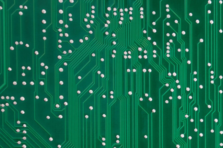
How to reduce high-speed PCB crosstalk?
Nov 27, 2021The influence of crosstalk in PCBs has always existed, especially in some high-speed and high-density PCBs. So how should we reduce crosstalk? The most basic thing is to make the coupling between the interfering network and the interfered network smaller, so it is almost impossible to completely avoid it in the design. When designing, we can only consider that it will not affect its performance, and choose the appropriate method to minimize it. Mainly consider from the following aspects:

1. Maximize the distance between transmission lines when wiring; or reduce the parallel length between adjacent transmission lines as much as possible, and try to run between different layers.
2. Because the wiring directions of two adjacent signal layers are vertical, try to avoid parallel wiring and reduce crosstalk between layers.
3. Under the condition of ensuring signal timing, try to choose devices with low conversion speed as much as possible to slow down the rate of change of electric and magnetic fields, thereby reducing crosstalk.
4. Since the surface layer has only one reference plane, the electric field coupling of the surface layer wiring is stronger than that of the middle layer, so the signal lines sensitive to crosstalk should be distributed in the inner layer as much as possible.