Flex PCB Design
February 17 , 2022
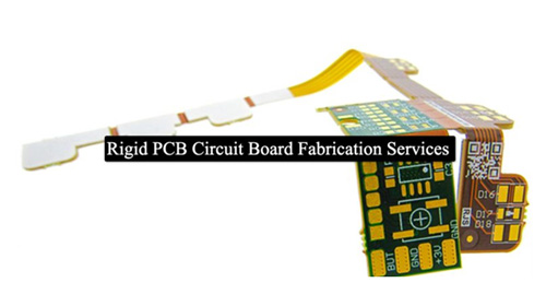
Flexible PCB
design requires a slightly different approach than rigid PCBs. While flexible
PCBs can offer significant manufacturing cost savings, reduced space
consumption, and reduced weight compared to rigid, their designs must be
optimized for their materials and use cases.
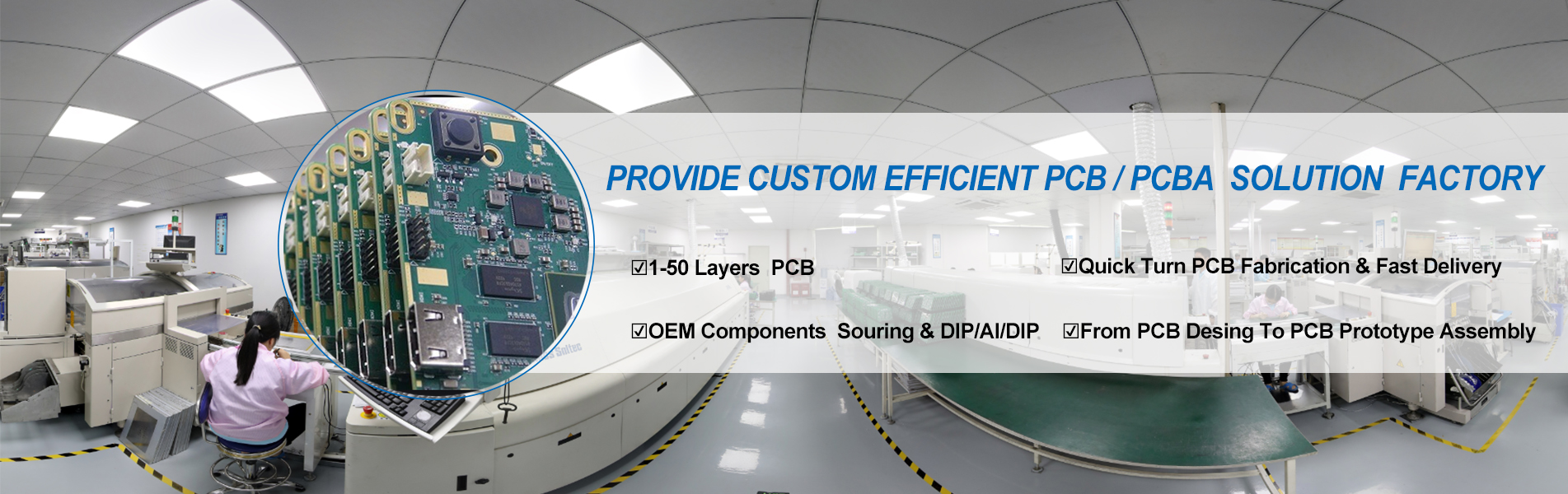
Using Cadence's suite of design and analysis tools in flex pcb design certainly provides any flex PCB prototype you may need in your design. Getting all the help you need, especially in the form of OrCAD PCB Designer, is the key to minimizing early problems in flex PCB prototypes. 10 steps to pay attention to:
Learn about electrical parameters.
2. Create a schematic.
3. Use the schematic capture tool to create your PCB layout.
4. Design your flex PCB stackup.
5. Define design rules and requirements.
6. Place the components.
7. Insert the drilled hole.
8. Wiring.
9. Add labels and identifiers.
10. Generate design/layout files


 English