PCB via analysis
Jun 23, 2021
Every hole on the PCB can be called a via. It is one of the important components of multilayer PCB. Let's get to know the knowledge of vias together.
Drill a common hole, that is, a via hole, at the intersection of the wires that need to be connected to each layer of the double-sided or multi-layer board. In terms of function, it is used as the electrical connection between the various layers of the PCB; and the other is used as the fixation or positioning of the device.
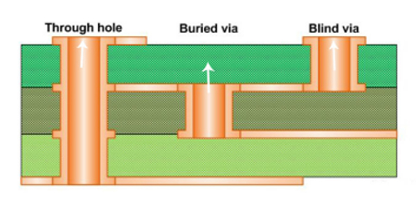
In terms of process, via holes are divided into three types: blind holes, buried holes, and through holes. Blind holes are through holes that connect the surface and inner layers without going through the entire board, and are used to connect and conduct two or more layers of PCB. The copper foil lines between, because all the layers are not drilled, only the top layer or the bottom layer can be seen. Buried holes are connecting holes in the inner layer of the PCB. They are used to interconnect any circuit on the inner layer, but they do not extend to the surface of the circuit board, so the surface and bottom layers are invisible. There is also a through hole, which passes through The whole PCB can realize the conductive connection between different layers or the installation and positioning of components.

In the design of vias, the size, quantity and spacing of vias must be designed after comprehensive consideration and the manufacturing process, structural reliability, performance and other issues must be taken into account. For example, factors such as current and wiring must be considered. For some high-speed or high-density products, the smaller the via hole is the better, so that more wiring space can be reserved on the board, thereby increasing the wiring density. In addition, the smaller the via hole, the smaller its own parasitic capacitance, which is more suitable for high-speed circuits. However, limited by technology such as drilling and electroplating, the smaller the hole, the longer it takes to drill and the easier it is to deviate from the center position. And when the depth of the hole exceeds 6 times the drill diameter, the hole cannot be guaranteed The wall can be plated with copper uniformly. For the vias of the power supply or the bottom line, consider a larger size to reduce the impedance, and drill multiple holes in parallel to reduce the equivalent inductance. The spacing between vias and vias should also be avoided. If the spacing is too small, it is easy to cause holes when drilling.