PCBA
  • A good PCBA training
    May 23, 2021 A good PCBA training
    May 15, 2021, in order to let our newly joined our company staffs quickly familiarize themselves with the products and better serve every customer.  Mainly explain in detail about PCBA product identification. The engineer conducts a detailed analysis with his 10 years of experience in the PCBA industry and a series of PCBA products that the company has done. How should we identify PCBA? First of all, we need to understand the role of components on the PCBA board. For example: On the PCB, character“R” represents resistance, and its main function is to step down and divide the voltage. Character “C” represents the capacitance, and its main function on the PCB is to reduce noise and stabilize the voltage. The most important thing is the chip (IC), which is the most important part of the entire PCB, equivalent to the human brain. It integrates a variety of electronic components on the PCB to achieve a specific function of the circuit module. Its function is calculation and storage. How to ensure the quality of our products? The engineer takes the bluetooth audio PCBA as an example: in order to increase the service life of the product. PCBA is a key part of the electronic product. We know that the audio is in a long-term vibration state. This will have a great impact on our chips for a long time, so that the life of the electronic products will be shortened. We can dispensing the chip to help the chip be fixed in board. If you want to know more details, please contact us! Tel: +86 0755 2322 6243 EXT 801.
    View More
  • Determinants of solder-ability
    May 17, 2021 Determinants of solder-ability
    In the process of PCBA processing, solder-ability directly affects the quality of the electronic product. Some inadvertent small problems can affect the solder-ability of the product. In order to avoid such problems, we must understand first. PCBA solder-ability is actually the PCBA soldering effect, which can be summarized as 4 major factors: 1. The quality of the PCB The manufacturing process and size design of the PCB all affect the solder-ability of the PCBA. For example, if the PCB size is too small, the soldering will be difficult to control and mutual interference will occur, so the design directly affects the soldering. How to avoid controlling the quality of incoming materials and ensuring that the supplier has done solder-ability testing to reduce this risk. 2. Solder paste The factor of solder paste also plays a important role in the solder-ability of PCBA. Pay attention to the storage time of solder paste and defrost it after opening. After thawing, stir the solder paste again. It is best to use it up on the same day and change the solder paste frequently. Steel mesh. 3. Components The components are assembled on the PCB. If you don’t pay attention to the storage time and environment of the components, and you don’t pay attention to avoiding damp and oxidation, it will be easy to short-circuit and crack during soldering. Also, it is to control incoming materials to test its solder-ability to ensure production. When the problem occurs. 4. Production environment The temperature and humidity of the workshop cannot be too high or too low. High humidity will affect the solder paste to cause bridging during reflow, and excessive water absorption will cause poor aggregation. Low humidity directly affects the flux evaporation rate, causing the solder paste to dry out and affect soldering. The high temperature reduces the viscosity of the solder paste and can also cause additional oxidation of the solder and affect the solder-ability. Low temperature can cause bad printing behavior, so the temperature and humidity of the environment are also extremely important. Pay attention to the temperature and humidity of the workshop is also the key point that can determine the solder-ability factor. Controlling these four determinants of weld-ability in the production process can effectively improve PCBA product quality.
    View More
  • What is ENIG?
    April 23, 2021 What is ENIG?
    ENIG full name is Electroless Nickel/Immersion Gold(some people call Chemical nickel gold, immersion nickel gold and soft gold) It is a continuous layer of nickel-gold alloy deposited on the surface of copper through redox reaction, a process of applying solderable coating on the bare copper surface of the PCB, which makes the PCB have better electrical conductivity and prolongs the service life of the PCB. Sometimes the cost of this surface treatment process will account for 20% of the cost of the printed circuit board. In actual production applications, 90% of the gold plates use the process of ENIG. After this process, the color of the PCB surface is stable to golden yellow,the brightness is good, the plating layer is flat, and the thickness of the surface treatment as the pad is generally 0.03µ - 0.08 µ. In the same way, gold finger PCB is made. Compared with the Gold Plating process, the gold finger of ENIG is not wear-resistant.If you do not often plug and unplug the Golden finger , you can also choose ENIG Process. At present, about 10%-20% of PCBs surface treatment use ENIG. The first choice for the button PCB, suitable for the edge connection area of the router shell and the electrical contact area for elastic connection of the chip processor, high-precision PCB with bonding IC, or BGA design. (1)Functions: ENIG makes the welding surface flat and can be well welded. Compared with Gold Plating, it has a lower cost and can prevent corrosion on the exposed copper surface. (2)Advantage: a). PCB surface is flat, good coplanarity b). The solderability is good, and the soldering of the components is stronger (over reflow soldering will not affect its solderability) c). It is not easy to be oxidized and anti-corrosion, so that the PCB can be stored for a longer time (3)Disadvantage: a). Compared with Gold Plating, the ENIG process is not wear-resistant b). Compared with the OSP process, the ENIG process is complicated General ENIG process: Acid cleaning→micro-etching→pre-dipping→activation→electroless nickel plating→chemical immersion gold. Comparison of ENIG and Plating Gold: Outward Appearance Solderability Antioxidant capacity Solder mask Binding force Plating Gold Bias towards white ★★ ★★★ ★★ ENIG Bias towards yellow ★★★ ★★★★★★ ★★★
    View More
  • What is HASL?
    April 09, 2021 What is HASL?
    HASL,Hot-air solder leveling (also somebody call spray tin), a process in which lead-tin solder is applied (melted) on the surface of the PCB, and the lead-tin solder is blown flat with heated compressed air. (In the dynamic environment of high temperature and high pressure, the PCB is immersed in the lead-tin solder (melted), and the air knife will flatten the liquid solder on the copper surface) The HASL process is relatively dirty, smells bad, and is relatively dangerous, and the technical control is relatively complicated. If the flatness is not good, it will affect the welding quality of the components. With the advancement of technology, a HASL process suitable for assembling QFP and BGA with a smaller pitch has also emerged. In actual applications, OSP and ENIG are both selected. At present, in PCB surface treatment, 20% -40% will use hot air leveling, let us understand its advantages and disadvantages together. (1). Function: The lead-tin solder (melted) forms a layer of anti-copper oxidation coating, slows the oxidation of copper, and forms a copper-tin metal compound (about 1 to 2 mils in thickness) at the junction with copper, providing good solder-ability. (2). Advantages and disadvantages of hot air leveling: Advantage: a) Low cost, good solder-ability b) Fully cover the side edge of the wire c) Avoid corrosion disconnection on the printed board (3).Disadvantages: a) Poor surface flatness b) The tin beads produced are easy to short-circuit the components of the fine-gap pins c) The PCB is prone to warp due to large thermal shock. (4). General process: Micro-etching→preheating→coating flux→spraying tin→cleaning. Tin spray is divided into lead-free spray tin (lead content less than&nbs...
    View More
  • How to inspect PCBA incoming materials?
    March 25, 2021 How to inspect PCBA incoming materials?
    The empty PCB board assembles various electronic components on the circuit board through SMT, and then forms PCBA through DIP plug-in. Among them, the incoming components are in the SMT inspection process. We need to check whether the labels and model specifications of the incoming materials are consistent. Use a magnifying glass to check whether the physical model specifications and silk-screen logos are consistent. Check the structure and shape after the model and silk-screen are no problem. It is consistent with the drawings and samples in the acknowledgment. Refer to the drawings and use a vernier to measure the size of the chip capacitors to meet the requirements. We need to use a digital bridge (LCR METER) tester to select DCR for testing. The capacity should be within the required range when measuring the capacity, and the loss value should be recorded while measuring the capacity, and the value should be within the required range. After passing the above inspections, the chip capacitors can be placed in the machine for placement, the components are soldered on the PCB board through the placement machine (SMT), manual welding (DIP, AI) and other equipment methods. A wide variety of chip capacitors is just one of them. It is a component that can store charges, and the same component has different dielectric specifications, and different specifications have different characteristics and uses. There are also diodes, tertiary tubes, and stickers. Chip resistors, various IC chips, relays, transformers, etc., they play their due role on the PCBA. If you want to know more about the detailed inspection standards of PCBA components, please call us: +86 0755 2322 6243 EXT 801. info@xlpcba.com+86 0755-2322 6243 EXT
    View More
  • The Computer Motherboard PCB Assemble
    June 05, 2020 The Computer Motherboard PCB Assemble
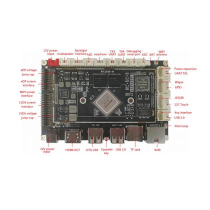
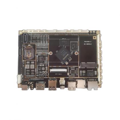
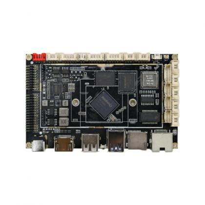
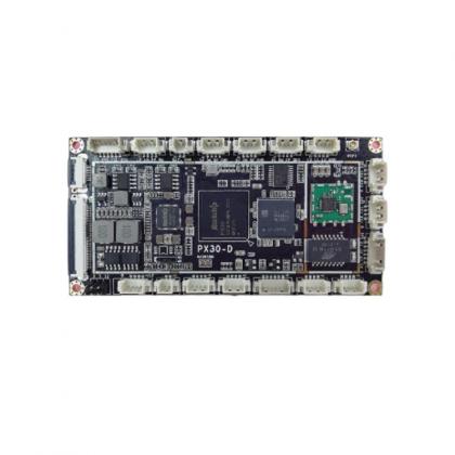
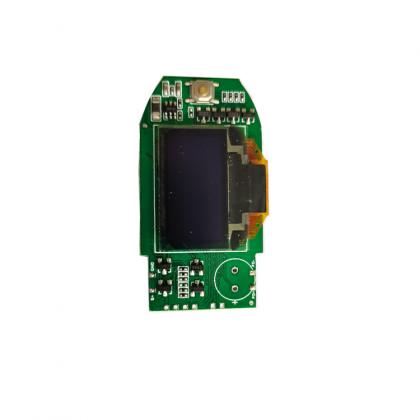
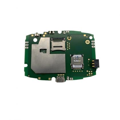
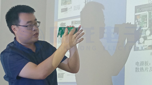
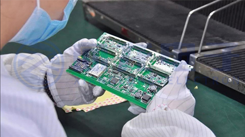
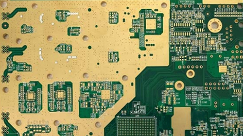
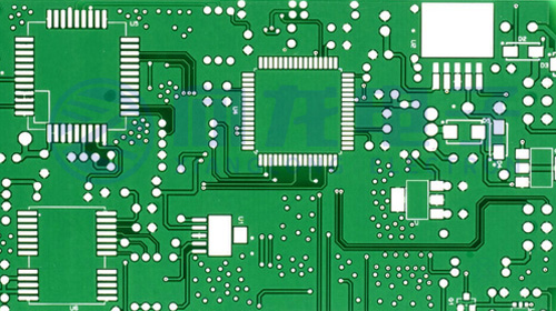
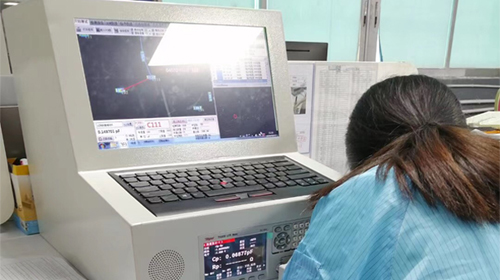
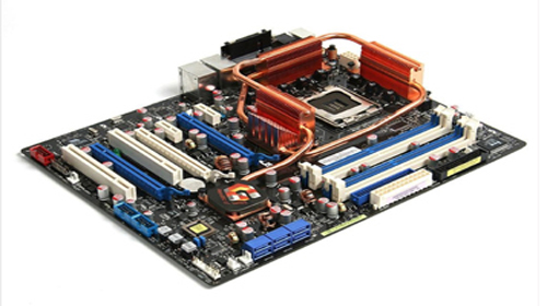
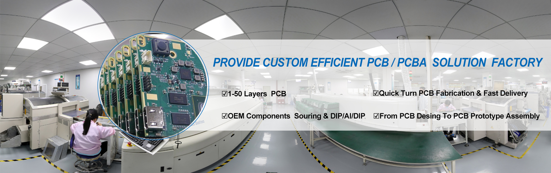
    How do we assemble the computer motherboard PCB? Put the produced PCB on the SMT automated production line, put a steel mesh on the automatic paste brushing machine, after the automatic paste brushing machine, it will brush a layer of solder paste on the corresponding position of the computer motherboard PCB, high-speed machine (similar to Intelligent robot) Assemble rice-sized capacitors and resistors on the computer motherboard PCB. The general-purpose machine attaches IO sound card chips, network card chips, power management chips, south bridge, north bridge chips, field effect transistors and other components to the PCB, although it is There are robots, but there will still be skilled operators operating and checking on the line. QC strictly supervises and checks the quality in accordance with the ISO9001 standard to ensure that the components will not be installed incorrectly or missed or installed incorrectly, and flow into the reflow furnace. This process will solder all the previously attached components. After that, it will be inspected by automatic optical inspection machine (AOI) and ICT, mainly for appearance inspection. Whether the stickers are reversed or crooked, the pictures taken are checked against the database to ensure that each component is completely correct. Whether the circuit function is normal. The inspected qualified products will be sent to the DIP production workshop. The DIP production line is filled with fixtures. This is used to fix the computer motherboard PCBA. Skilled operators will install relatively large memory slots, PCI slots, and AGPs on it. Slots, various interfaces, audio connectors and other components, after completion, perform ICT testing (can the motherboard be lit, whether the function is normal), we also call FQC testing, if it is a qualified product, it can be packed in an anti-static bag. Packaging standard: the keyboard and mouse interface is facing right, and the sealing is to the welding surface. Put it in the box together with the accessories, and the box will be pulled to the warehouse. If it fails, it will be repaired or scrapped directly. Please give us the authorization letter before signing the PCBA contract for manufacturing computer motherboards. We will strictly follow the quality requirements and manufacturing standards specified in the contract to manufacture and deliver on time. If you want to know more about the PCB manufacturing and assembly services provided by Xianglong (Shenzhen) Electronic Technology Co., Ltd. for computer motherboard PCBA and computer peripheral products, please call +86 0755 2322 6243 EXT 801. You can also email your specifications to info@xlpcba.com
    View More
  • FPC Market Prospects And Trends
    August 28, 2020 FPC Market Prospects And Trends
    Flexible printed circuit boards have the characteristics of light weight and thin thickness. Compared with rigid printed circuit boards, it can save up to 60% of space and weight. In addition, the benefits provided in terms of durability and cost further expand their adoption rates in different end-use industries. At present, FPC has been widely used in mobile smart terminals such as smart phones, tablet computers, and wearable devices. It is the only solution to meet the needs of miniaturization and convenient movement of electronic products. In recent years, the flexible PCB market technology has undergone major changes from the traditional single-sided flexible circuit to the advanced multilayer flexible circuit board. The rise of rigid-flex circuit technology is creating great potential in various telecommunications and medical applications, and driving the demand for flexible PCB technology. In the flexible PCB market, various technologies such as single-sided, double-sided, multilayer and rigid flexible circuits are used in various applications. The growing demand for FPC in the telecommunications industry, the growth of connected devices and the advancement of automotive electronics technology have created new opportunities for various flexible PCB technologies.
    View More
  • What is PCB?
    October 08, 2020 What is PCB?
    PCB, as the "mother of electronic products", is a bridge that carries electronic components and connects circuits. It is widely used in communications, consumer electronics, computers, automotive electronics, industrial control, medical equipment, national defense, aerospace and other fields. It is a modern electronics indispensable electronic components in information products. It is a provider of electrical connections for electronic components. The downstream of the PCB industry covers almost all electrical circuit products, and the core applications with the largest output value include communication equipment, computers, consumer electronics and automotive electronics. With the development of electrification and automation in human society, the application range of PCB is becoming wider and wider, and there are no other substitutes for the time being. 1. Classification according to the strength of PCB substrate (1) Rigid printed boards Printed boards made of rigid substrates; (2) Flexible printed boards Printed boards made of flexible substrates, also known as flexible printed boards; (3) Rigid and flexible printed boards are printed boards made by using flexible substrates and combining them with rigid substrates in different areas. 2. Classification according to the method of making conductive patterns on PCB circuit boards (1) Subtractive PCB Printed circuit boards made by subtractive technology; (2)Additive PCB Printed circuit boards produced by the additive process. 3. According to the PCB circuit board substrate classification (1)Organic printed boards. Conventional printed boards are all organic printed boards, which are mainly composed of three materials: resin, reinforcing materials and copper foil. Resin materials include phenolic resin, epoxy resin, polyimide, /A resin, etc.; (2)Inorganic printed boards are commonly referred to as thick film circuits, which are composed of ceramics, metal aluminum and other materials. Inorganic printed boards are widely used in high-frequency electronic instruments. 4. Classification according to the conductive structure of the PCB circuit board (1)Single-sided printed circuit board refers to a printed circuit board with conductive patterns on only one side. Because the wires only appear on one side, this kind of printed circuit board is called a single-sided printed circuit board. (Referred to as single panel) (2)A printed board with conductive patterns on both sides of the double-sided printed board, because the area of the double-sided board is twice as large as that of the single-sided board, and the wiring can be staggered (it can be wound to the other side), which is more suitable for more complex On the circuit. (3)Multi-layer printed board A printed board made of 3 or more layers of conductive patterns and insulating materials alternately bonded together and laminated, referred to as a multilayer board, requires the conductive patterns between layers to be connected to each other as needed...
    View More
1 2 3 4

A total of 4 pages

Subscribe for our newsletter

Please read on, stay posted, subscribe, and we welcome you to tell us what you think.

click here to leave a message

Get a quote
If you need to send file or forms, please contact us by email info@xlpcba.com directly.

Home

Products

about

contact